- 您现在的位置:买卖IC网 > Sheet目录2004 > LTC1690IS8#TRPBF (Linear Technology)IC RCVR/DVR PAIR LOW PWR 8-SOIC
7
LTC1690
SWITCHI G TI E WAVEFOR S
UW
W
–VO
D
3V
0V
tPLH
VO = V(A) – V(B)
VO
Z
Y
tSKEW
tr
f = 1MHz, tr ≤ 10ns, tf ≤ 10ns
1.5V
90%
10%
50%
tPHL
tf
1.5V
90%
10%
50%
VO
1/2 VO
1690 F04
Figure 4. Driver Propagation Delays
f = 1MHz, tr ≤ 10ns, tf ≤ 10ns
NOTE: tSKD = |tPHL – tPLH|
INPUT
OUTPUT
A – B
R
VOD2
–VOD2
5V
VOL
tPHL
0V
1.5V
tPLH
0V
1.5V
1690 F05
Figure 5. Receiver Propagation Delays
FUNCTION TABLES
UU
Driver
DZ
Y
101
010
Receiver
A – B
R
≥ –0.01V
1
≤ –0.20V
0
Inputs Open
1
Inputs Shorted
1
Note: Table valid with or without termination resistors.
1690 F01
Y
Z
R
VOD2
VOC
1690 F02
Y
Z
60
375
VOD3
VTST
–7V TO 12V
375
1690 F03
D
Y
Z
RDIFF
A
B
15pF
CL1
CL2
R
+
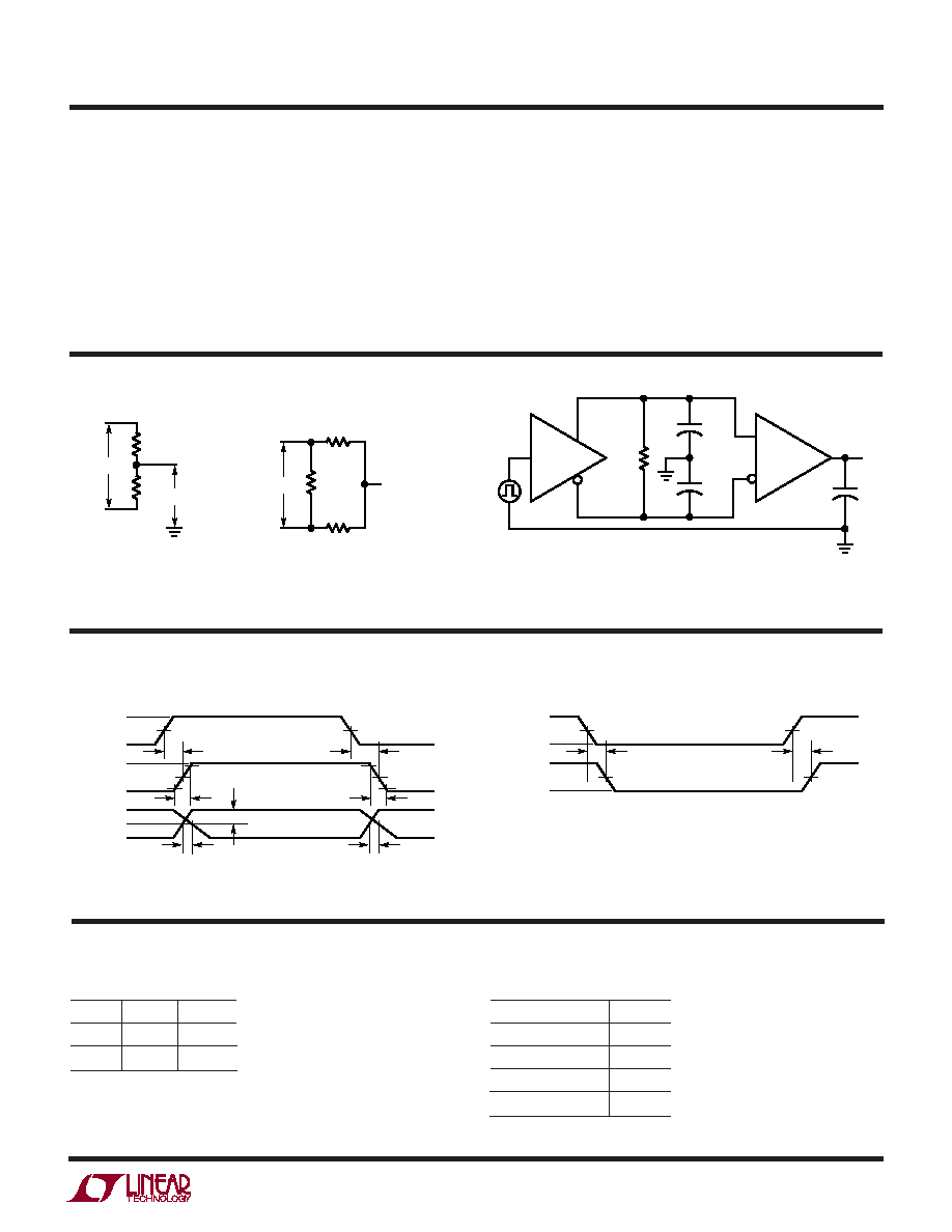
Figure 1. Driver
DC Test Load #1
Figure 2. Driver
DC Test Load #2
Figure 3. Driver/Receiver
Timing Test Load
TEST CIRCUITS
PIN FUNCTIONS
UU
U
VCC (Pin 1): Positive Supply. 4.75V < VCC < 5.25V.
R (Pin 2): Receiver Output. R is high if (A – B)
≥ –10mV
and low if (A – B)
≤ –200mV.
D (Pin 3): Driver Input. If D is high, Y is taken high and Z
is taken low. If D is low, Y is taken low and Z is taken high.
GND (Pin 4): Ground.
Y (Pin 5): Driver Output.
Z (Pin 6): Driver Output.
B (Pin 7): Receiver Input.
A (Pin 8): Receiver Input.
发布紧急采购,3分钟左右您将得到回复。
相关PDF资料
LTC1740IG#TRPBF
IC ADC 14BIT 6MSPS 36SSOP
LTC1741IFW#PBF
IC ADC 12BIT 65MSPS 48-TSSOP
LTC1742CFW#TRPBF
IC ADC 14BIT 65MSPS 48-TSSOP
LTC1743IFW#PBF
IC ADC 12BIT 50MSPS SMPL 48TSSOP
LTC1744IFW#TRPBF
IC ADC 14BIT 50MSPS 48-TSSOP
LTC1745CFW#TRPBF
IC ADC 12BIT 25MSPS LN 48TSSOP
LTC1746IFW#TRPBF
IC ADC 14BIT 25MSPS LP 48TSSOP
LTC1747IFW#PBF
IC ADC 12BIT 80MSPS 48-TSSOP
相关代理商/技术参数
LTC1690IS8PBF
制造商:Linear Technology 功能描述:Differential Driver/Receiver Pair SOIC8
LTC1693-1CS8
功能描述:IC MOSFET DVR N-CH DUAL 8-SOIC RoHS:否 类别:集成电路 (IC) >> PMIC - MOSFET,电桥驱动器 - 外部开关 系列:- 标准包装:5 系列:- 配置:低端 输入类型:非反相 延迟时间:600ns 电流 - 峰:12A 配置数:1 输出数:1 高端电压 - 最大(自引导启动):- 电源电压:14.2 V ~ 15.8 V 工作温度:-20°C ~ 60°C 安装类型:通孔 封装/外壳:21-SIP 模块 供应商设备封装:模块 包装:散装 配用:BG2A-NF-ND - KIT DEV BOARD FOR IGBT 其它名称:835-1063
LTC1693-1CS8#PBF
功能描述:IC MOSFET DVR N-CH DUAL 8-SOIC RoHS:是 类别:集成电路 (IC) >> PMIC - MOSFET,电桥驱动器 - 外部开关 系列:- 标准包装:95 系列:- 配置:高端和低端,独立 输入类型:非反相 延迟时间:160ns 电流 - 峰:290mA 配置数:1 输出数:2 高端电压 - 最大(自引导启动):600V 电源电压:10 V ~ 20 V 工作温度:-40°C ~ 125°C 安装类型:表面贴装 封装/外壳:8-SOIC(0.154",3.90mm 宽) 供应商设备封装:8-SOIC 包装:管件 产品目录页面:1381 (CN2011-ZH PDF)
LTC1693-1CS8#TR
功能描述:IC DRVR MOSF DUAL N-CH HS 8SOIC RoHS:否 类别:集成电路 (IC) >> PMIC - MOSFET,电桥驱动器 - 外部开关 系列:- 标准包装:5 系列:- 配置:低端 输入类型:非反相 延迟时间:600ns 电流 - 峰:12A 配置数:1 输出数:1 高端电压 - 最大(自引导启动):- 电源电压:14.2 V ~ 15.8 V 工作温度:-20°C ~ 60°C 安装类型:通孔 封装/外壳:21-SIP 模块 供应商设备封装:模块 包装:散装 配用:BG2A-NF-ND - KIT DEV BOARD FOR IGBT 其它名称:835-1063
LTC1693-1CS8#TRPBF
功能描述:IC MOSFET DVR N-CH DUAL 8-SOIC RoHS:是 类别:集成电路 (IC) >> PMIC - MOSFET,电桥驱动器 - 外部开关 系列:- 标准包装:5 系列:- 配置:低端 输入类型:非反相 延迟时间:600ns 电流 - 峰:12A 配置数:1 输出数:1 高端电压 - 最大(自引导启动):- 电源电压:14.2 V ~ 15.8 V 工作温度:-20°C ~ 60°C 安装类型:通孔 封装/外壳:21-SIP 模块 供应商设备封装:模块 包装:散装 配用:BG2A-NF-ND - KIT DEV BOARD FOR IGBT 其它名称:835-1063
LTC1693-1IS8
功能描述:IC MOSFET DVR N-CH DUAL 8-SOIC RoHS:否 类别:集成电路 (IC) >> PMIC - MOSFET,电桥驱动器 - 外部开关 系列:- 标准包装:5 系列:- 配置:低端 输入类型:非反相 延迟时间:600ns 电流 - 峰:12A 配置数:1 输出数:1 高端电压 - 最大(自引导启动):- 电源电压:14.2 V ~ 15.8 V 工作温度:-20°C ~ 60°C 安装类型:通孔 封装/外壳:21-SIP 模块 供应商设备封装:模块 包装:散装 配用:BG2A-NF-ND - KIT DEV BOARD FOR IGBT 其它名称:835-1063
LTC1693-1IS8#PBF
功能描述:IC MOSFET DVR N-CH DUAL 8-SOIC RoHS:是 类别:集成电路 (IC) >> PMIC - MOSFET,电桥驱动器 - 外部开关 系列:- 标准包装:95 系列:- 配置:高端和低端,独立 输入类型:非反相 延迟时间:160ns 电流 - 峰:290mA 配置数:1 输出数:2 高端电压 - 最大(自引导启动):600V 电源电压:10 V ~ 20 V 工作温度:-40°C ~ 125°C 安装类型:表面贴装 封装/外壳:8-SOIC(0.154",3.90mm 宽) 供应商设备封装:8-SOIC 包装:管件 产品目录页面:1381 (CN2011-ZH PDF)
LTC1693-1IS8#TR
功能描述:IC DRVR MOSF DUAL N-CH HS 8SOIC RoHS:否 类别:集成电路 (IC) >> PMIC - MOSFET,电桥驱动器 - 外部开关 系列:- 标准包装:5 系列:- 配置:低端 输入类型:非反相 延迟时间:600ns 电流 - 峰:12A 配置数:1 输出数:1 高端电压 - 最大(自引导启动):- 电源电压:14.2 V ~ 15.8 V 工作温度:-20°C ~ 60°C 安装类型:通孔 封装/外壳:21-SIP 模块 供应商设备封装:模块 包装:散装 配用:BG2A-NF-ND - KIT DEV BOARD FOR IGBT 其它名称:835-1063